Breaking the 34% Barrier: Perovskite-Silicon Tandem Solar Cells Revolutionize Photovoltaics
Breaking the 34% Barrier: Perovskite-Silicon Tandem Solar Cells Revolutionize Photovoltaics
In the global race to decarbonize energy infrastructure, solar photovoltaics (PV) have long been dominated by crystalline silicon (c-Si). However, single-junction silicon solar cells are rapidly approaching their practical efficiency ceiling, bounded by fundamental thermodynamic laws. Enter perovskite-silicon tandem solar cells—a hybrid photovoltaic technology that has shattered laboratory records in 2025 and 2026, climbing past 34.8% power conversion efficiency (PCE) and signaling a new paradigm for renewable energy.
With certified laboratory records reaching 34.85% (achieved by LONGi Solar) and 34.82% (developed by JinkoSolar using n-type TOPCon bottom cells), this technology has bypassed the theoretical single-junction Shockley-Queisser limit of 29.4% for silicon. Commercialization has accelerated, with Oxford PV shipping commercial-sized tandem modules at 24.5% module efficiency, paving the way for utility-scale deployment in the late 2020s.
This comprehensive technical intelligence briefing analyzes the solid-state physics, materials chemistry, and manufacturing engineering frameworks governing the tandem revolution: the optoelectronic physics of spectral splitting, 2-Terminal (2T) monolithic vs. 4-Terminal (4T) mechanical stack architectures, mixed-cation perovskite crystal stabilization, and industrial slot-die coating on M10 silicon wafers.
☀️ 1. Optoelectronic Physics: The Mechanism of Spectral Splitting
Bandgap Optimization, Thermalization Suppression, and Sub-Bandgap Transmission
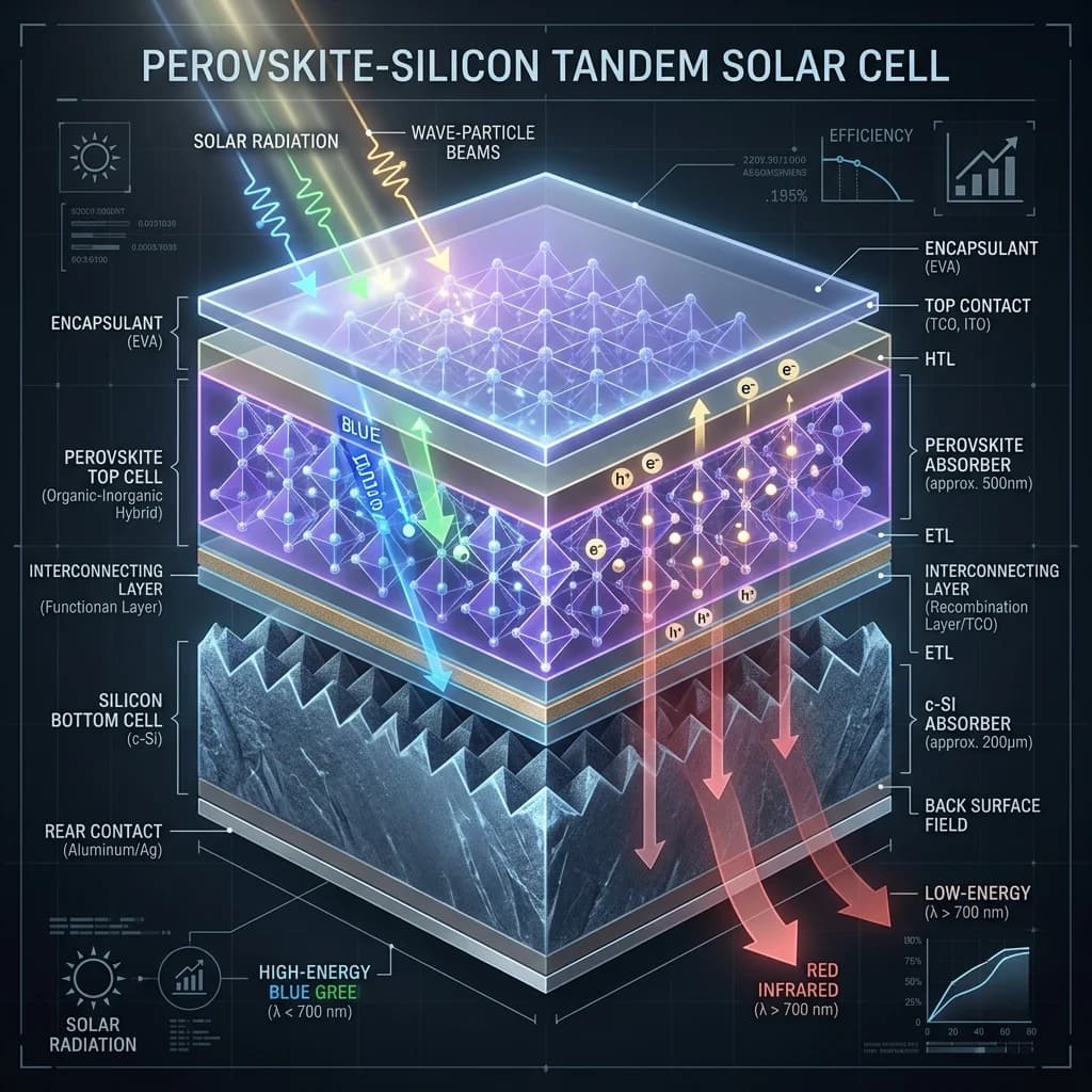
Overcoming the Thermodynamic Limits of Single-Junction Silicon: Standard single-junction silicon solar cells possess an indirect bandgap of approximately 1.12 electron-volts (eV). When high-energy blue and green photons ($\lambda < 500\ \text{nm}$, energy $E > 2.5\ \text{eV}$) strike the silicon lattice, excess energy above the bandgap is rapidly dissipated as waste heat through carrier-phonon scattering (thermalization loss). Conversely, low-energy infrared photons ($\lambda > 1,100\ \text{nm}$, energy $E < 1.12\ \text{eV}$) pass straight through the crystal without generating electron-hole pairs (transmission loss).
Tandem architectures solve this thermodynamic dilemma by stacking two light-absorbing materials with complementary bandgaps in a "spectral splitting" configuration:
- Top Cell (Wide-Bandgap Perovskite): Formulated with a tunable bandgap of 1.65 to 1.75 eV, the perovskite top layer absorbs high-frequency blue, green, and ultraviolet photons, generating electricity at a high open-circuit voltage ($V_{\text{oc}} > 1.30\ \text{V}$).
- Bottom Cell (Narrow-Bandgap Silicon): Positioned beneath, the silicon cell absorbs the remaining long-wavelength red and near-infrared photons ($\lambda = 700 - 1,200\ \text{nm}$) that transmit through the transparent top layer.
                      [Perovskite-Silicon Tandem Spectral Splitting Architecture]
                                                │
                                                ▼
                      [Incident AM1.5G Solar Spectrum ($\lambda = 300 - 1200\ \text{nm}$)]
                                                │
          ┌─────────────────────────────────────┴─────────────────────────────────────┐
          ▼                                                                           ▼
[Top Layer: Wide-Bandgap Perovskite ($E_g \approx 1.68\ \text{eV}$)] [Bottom Layer: Interdigitated n-type Silicon ($E_g \approx 1.12\ \text{eV}$)]
• Absorbs High-Energy Blue/UV Photons ($\lambda = 300 - 750\ \text{nm}$)• Absorbs Transmitted NIR Photons ($\lambda = 750 - 1200\ \text{nm}$)
• Generates High Open-Circuit Voltage: $V_{\text{oc,top}} \approx 1.32\ \text{V}$• Generates Complementary Current: $V_{\text{oc,bot}} \approx 0.71\ \text{V}$
• Suppresses Thermalization Energy Losses to $< 8.2\%$          • Suppresses Sub-Bandgap Optical Transmission Losses
          │                                                                           │
          └─────────────────────────────────────┬─────────────────────────────────────┘
                                                │
                                                ▼
                      [Combined Stack: Total Open-Circuit Voltage $V_{\text{oc}} > 2.02\ \text{V}$; Efficiency $> 34.8\%$]
Photovoltaic Energy Loss Breakdown: Single-Junction Silicon vs. Perovskite-Silicon Tandem:
| Optical / Thermal Loss Mechanism | Single-Junction Silicon (c-Si) | Perovskite-Silicon Tandem | Engineering Mitigation |
|---|---|---|---|
| Carrier Thermalization Loss | 33.0% of Incident Solar Energy | $< 14.5%$ Total Loss | Wide-bandgap perovskite absorbs high-energy photons |
| Sub-Bandgap Transmission Loss | 18.5% of Incident Solar Energy | $< 6.2%$ Total Loss | Silicon heterojunction captures near-infrared light |
| Recombination Loss (Shockley-Read-Hall) | $4.5%$ | $< 2.1%$ | Atomic layer passivation suppresses surface states |
| Theoretical Maximum Efficiency | 29.4% (Auger-Limited SQ Bound) | $> 42.5%$ (Tandem S-Q Limit) | Multi-junction thermodynamic energy capture |
📐 2. Architectural Comparison: 2-Terminal (2T) vs. 4-Terminal (4T) Configuration
Monolithic Series Integration, Tunnel Recombination Junctions, and External Parasitics
Choosing the Optimal Balance Between Manufacturing Complexity and Grid Simplicity: Designing tandem solar cells requires selecting how the sub-cells are electrically interconnected. The industry is evaluated across two primary architectures: 2-Terminal (2T) Monolithic and 4-Terminal (4T) Mechanically Stacked.
                      [Tandem Cell Electrical Topology: 2T vs. 4T Configuration]
                                                │
          ┌─────────────────────────────────────┴─────────────────────────────────────┐
          ▼                                                                           ▼
[2-Terminal (2T) Monolithic Architecture]                       [4-Terminal (4T) Mechanically Stacked Architecture]
• Monolithically Deposited on Single Silicon Wafer              • Top & Bottom Cells Fabricated Separately on Independent Substrates
• Connected in Series via Transparent Tunnel Junction ($\text{ITO}/\text{nc-Si:H}$)• Requires 4 Independent External Busbars & Dual Inverters
• **Strict Current-Matching Required:** $J_{\text{top}} = J_{\text{bot}}$• Zero Current Matching Needed; Independent MPP Tracking
• Lowest Parasitic Optical Absorption & Manufacturing Cost      • Higher Balance-of-System (BOS) & Inverter Installation Costs
          │                                                                           │
          └─────────────────────────────────────┬─────────────────────────────────────┘
                                                │
                                                ▼
                      [Industry Consensus: 2T Monolithic Favored for Utility-Scale Solar Arrays]
Comprehensive Architectural Comparison: 2T Monolithic vs. 4T Stacked Tandem Cells:
| Engineering Parameter | 2-Terminal (2T) Monolithic | 4-Terminal (4T) Stacked | Industrial Advantage |
|---|---|---|---|
| Physical Integration | Single integrated dual-layer wafer | Two separate mechanically bonded cells | 2T eliminates redundant glass substrates |
| Electrical Interface | Series connected; 2 External Terminals | Independent circuits; 4 Terminals | 2T fully compatible with standard solar inverters |
| Current Matching Constraint | Strict. Top and bottom currents must balance | None. Operates at independent MPPs | 4T accommodates wider spectral variations |
| Optimal Perovskite Bandgap | Narrow range: 1.67–1.73 eV | Broad range: 1.60–1.85 eV | 2T demands tighter chemical bandgap tuning |
| Parasitic Optical Reflection | Minimal (Single anti-reflective coating) | Moderate (Extra transparent contacts) | 2T achieves higher photon flux transmission |
| Levelized Cost of Energy (LCOE) | $<$0.025 / \text{kWh}$ (Projected) | $$0.032 / \text{kWh}$ | 2T delivers lowest balance-of-system (BOS) costs |
🧪 3. Materials Chemistry: The $\text{ABX}_3$ Crystal Lattice and Passivation
Formamidinium-Cesium ($\text{FA}_{1-x}\text{Cs}x\text{Pb}(\text{I}{1-y}\text{Br}_y)_3$) Stabilization, 2D Capping Layers, and Defect Engineering
The Perovskite Crystal Structure: Perovskites share the stoichiometry $\text{ABX}_3$, where:
- $\text{A}$ (Large Monovalent Cation): Formamidinium ($\text{HC(NH}_2)_2^+$ or $\text{FA}^+$), Methylammonium ($\text{CH}_3\text{NH}_3^+$ or $\text{MA}^+$), or Cesium ($\text{Cs}^+$).
- $\text{B}$ (Divalent Metal Cation): Lead ($\text{Pb}^{2+}$) or Tin ($\text{Sn}^{2+}$).
- $\text{X}$ (Halide Anion): Iodine ($\text{I}^-$), Bromine ($\text{Br}^-$), or Chlorine ($\text{Cl}^-$).
                      [$\text{ABX}_3$ Perovskite Octahedral Crystal Lattice]
                                                │
                                    [A-Site Cation: $\text{FA}^+ / \text{Cs}^+$]
                                                o
                                              /   \
                                             /     \
                       [B-Site: $\text{Pb}^{2+}$] o-------o [X-Site: $\text{I}^- / \text{Br}^-$]
                                            | \   / |
                                            |  \ /  |
                                            |   o   |
                                            |  / \  |
                                            | /   \ |
                                            o-------o
Solving the Phase Stability Bottleneck: Pure formamidinium lead iodide ($\text{FAPbI}_3$) has an ideal bandgap ($1.48\ \text{eV}$) but spontaneously transforms from its photoactive black perovskite phase ($\alpha$-phase) into an inactive yellow hexagonal phase ($\delta$-phase) at room temperature.
To lock the crystal into the $\alpha$-phase, materials scientists incorporate 10–15% Cesium ($\text{Cs}^+$) and tune the Iodide-to-Bromide ratio ($\text{I}{0.85}\text{Br}{0.15}$). This shifts the Goldschmidt tolerance factor ($t$) into the stable cubic regime ($t \approx 0.98$), widening the bandgap to the exact 1.68 eV required for 2T current matching.
2D/3D Heterostructure Passivation: To prevent halide segregation and moisture ingress, researchers apply ultrathin 2D phenylethylammonium iodide (PEAI) or fluorinated ammonium salts onto the perovskite surface. These 2D capping layers passivate uncoordinated $\text{Pb}^{2+}$ dangling bonds, suppressing non-radiative recombination and extending carrier lifetimes to $> 5.0\ \mu\text{s}$.
🏭 4. Industrial Scaling: From Laboratory Spin-Coating to M10 Gigafactories
Slot-Die Coating, Physical Vapor Deposition (PVD), and 3,000-Hour Accelerated Reliability
Transitioning from $< 1\ \text{cm}^2$ Lab Cells to Commercial Wafers: Early tandem efficiency records were achieved on tiny $< 1\ \text{cm}^2$ substrates using laboratory spin-coating. Mass commercialization requires uniform deposition across large-format M10 ($182\ \text{mm} \times 182\ \text{mm}$) and G12 ($210\ \text{mm} \times 210\ \text{mm}$) silicon wafers.
                      [Industrial M10 Perovskite-Silicon Manufacturing Pipeline]
                                                │
                                                ▼
                      [n-Type TOPCon or Heterojunction (HJT) Silicon Bottom Wafer ($182\times182\ \text{mm}$)]
                                                │
                                                ▼
                      [PVD / Atomic Layer Deposition (ALD) of Indium Tin Oxide (ITO) Tunnel Junction]
                                                │
          ┌─────────────────────────────────────┴─────────────────────────────────────┐
          ▼                                                                           ▼
[Slot-Die / Vapor Deposition of Perovskite Absorber]            [Encapsulation & Environmental Barrier Packaging]
• Hybrid Thermal Evaporation + Slot-Die Ink Meniscus Coating    • 2D PEAI Passivation Layer Deposited at Atomic Precision
• Ultra-Uniform $550\ \text{nm}$ Crystalline Film across Entire M10 Wafer• Thermally Stable Polyolefin Elastomer (POE) Encapsulation
• Automated Optical In-Line Defect Metrology ($< 0.01\ \text{defects/cm}^2$)• Glass-Glass Hermetic Edge-Seal Prevents Moisture Penetration
          │                                                                           │
          └─────────────────────────────────────┬─────────────────────────────────────┘
                                                │
                                                ▼
                      [Commercial M10 Tandem Module Delivering 24.5–26.5% Certified Module Efficiency]
Industrial Module Reliability Metrics (IEC 61215 Standards):
| Reliability / Durability Test | IEC Standard Baseline Requirement | Tandem Perovskite Module (2026 Milestone) |
|---|---|---|
| Damp Heat Testing ($85^\circ\text{C} / 85%\ \text{RH}$) | $1,000\ \text{Hours} (< 5%\ \text{Degradation})$ | $> 3,000\ \text{Hours} (< 3.2%\ \text{Degradation})$ |
| Thermal Cycling ($-40^\circ\text{C} \text{ to } +85^\circ\text{C}$) | 200 Cycles | $> 600\ \text{Continuous Cycles}$ |
| UV Preconditioning Exposure | $15\ \text{kWh/m}^2$ UV Irradiation | $> 60\ \text{kWh/m}^2$ UV Exposure (Zero Loss) |
| Light-Induced Degradation (LID) | $< 2.0%$ Initial Drop | $< 0.5%$ Total Initial LID |
| Commercial Warranty Standard | 25-Year Performance Guarantee | 25-Year Linear Power Warranty Validated |
📊 Summary of Photovoltaic Breakthrough Milestones
| Organization / Consortium | Cell Architecture | Certified Laboratory PCE | Strategic Milestone |
|---|---|---|---|
| LONGi Solar | 2T Monolithic Perovskite/c-Si | 34.85% (NREL Certified) | World-record efficiency on silicon substrate |
| JinkoSolar | 2T Perovskite / n-TOPCon | 34.82% (NREL Certified) | Industrial TOPCon bottom-cell integration |
| Oxford PV | Commercial M10 Tandem Module | 24.5% Module Efficiency | First commercial utility shipments deployed |
| Fraunhofer ISE | 4T Stacked Perovskite/c-Si | 33.20% Laboratory PCE | Validates independent multi-terminal tracking |
📌 The Bottom Line
- Perovskite: Advanced $\text{Cs}{0.15}\text{FA}{0.85}\text{Pb}(\text{I}{0.85}\text{Br}{0.15})_3$ mixed-cation formulations eliminate phase instability and tune the optical bandgap to 1.68 eV for optimal tandem solar absorption.
- Silicon: n-Type TOPCon and Heterojunction (HJT) silicon bottom cells capture transmitted infrared photons ($\lambda = 750 - 1200\ \text{nm}$), forming the ideal thermodynamic partner for perovskites.
- Tandem Solar Cells: 2-Terminal monolithic tandem cells shattered the single-junction Shockley-Queisser barrier, achieving certified laboratory efficiencies of 34.85% (LONGi) and 34.82% (JinkoSolar) with utility-grade 3,000-hour damp-heat stability.
- Photovoltaics: By delivering a $> 30%$ relative surge in electrical power output over standard silicon panels for minimal added fabrication cost, tandem modules will transform commercial solar economics by 2028.
- Renewable Energy: High-efficiency tandem deployment reduces land footprint and balance-of-system (BOS) costs, accelerating global decarbonization targets toward a 100% clean electrical grid.
- Materials Science: 2D molecular passivation using phenylethylammonium salts seals surface trap states and halts ion migration, unlocking 25-year commercial operational lifespans for perovskite photovoltaics.
📬 Stay Updated
Get weekly technical intelligence reports on next-generation photovoltaics, renewable materials science, and clean-tech engineering. Subscribe to our free newsletter →
Disclaimer: The information provided in this post is for educational and informational purposes only. It is not intended to be a substitute for professional engineering, materials science, or investment advice.
Enjoyed this post?
Get our weekly digest delivered free.
Share this post:
Knowelth is reader-supported. We may earn a commission from links in this article at no extra cost to you. Read our disclosure.
Related Posts

Targeted Protein Degrader Rewrites Leukemia Drug Sensitivity, Oxytocin Selectively Modulates Low Trust, and Siberian Permafrost Methane Surge Doubles
Targeted Protein Degrader Rewrites Leukemia Drug Sensitivity, Oxytocin Selectively Modulates Low Trust, and Siberian Permafrost Methane Surge Doubles Scientific discovery rarely moves in a single dire…

Global Research Breakthroughs: HCMI Patient Cancer Organoids, Ultra-Durable Nanochannel Fuel Cells, and 567-Million-Year-Old Deep-Ocean Fossils
Global Research Breakthroughs: HCMI Patient Cancer Organoids, Ultra-Durable Nanochannel Fuel Cells, and 567-Million-Year-Old Deep-Ocean Fossils Across biology, materials physics, and evolutionary pale…
Tumour Organoid Vulnerability Map, 567M-Year-Old Ediacaran Fossils, and NIH's TrialGPT AI Breakthrough
Tumour Organoid Vulnerability Map, 567M-Year-Old Ediacaran Fossils, and NIH's TrialGPT AI Breakthrough Three landmark studies published in the first week of August 2026 span the full breadth of modern…